3-Layer High Frequency PCB Built on 60mil RO4350B and 6.6mil RO4350B with ENIG for Wireless Boosters
(Printed Circuit Boards are custom-made products; the images and parameters shown are for reference only.)
Introduction
Hello Everyone,
Today, we discuss a multilayer high-frequency PCB constructed entirely from high-frequency materials, including prepreg adhesive. For instance, a 4-layer RO4350B PCB consists of two cores of RO4350B substrates. The RO4350B family includes eight core thicknesses, ranging from 4mil (0.101mm) to 60mil (1.524mm).
RO4350B Thickness Options
Thickness (mil) |
Thickness (mm) |
4mil |
0.101mm |
6.6mil |
0.168mm |
10mil |
0.254mm |
13.3mil |
0.338mm |
16.6mil |
0.422mm |
20mil |
0.508mm |
30mil |
0.762mm |
60mil |
1.524mm |
So it’s very interesting that stack-up of 4 layers can be done in many different ways.
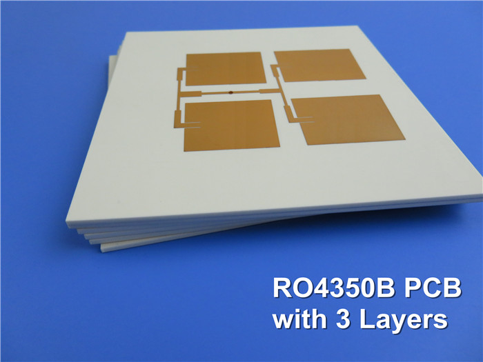
This 3-layer high-frequency PCB is built using two cores of RO4350B, with one copper layer etched away, resulting in three functional layers.
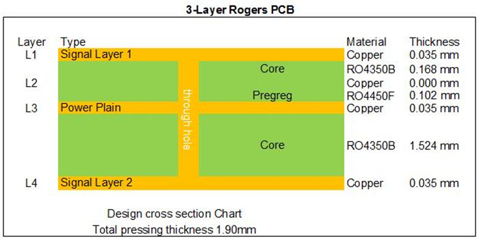
Structure and Specifications
The construction comprises one sheet of 60mil RO4350B, 4mil RO4450F prepreg, and a combined 6.6mil RO4350B. The board dimensions are 110mm x 110mm, featuring immersion gold finishes on the pads. Each order includes 20 pieces, designed specifically for wireless booster applications.
Following is the actual value in engineering manufacture.
Features and Benefits
1.Excellent High-Frequency Performance: Achieves low dielectric tolerance and loss.
2.Reduced Signal Loss: Meets the evolving demands of communication technology.
3.Professional Oversight: Experienced engineers verify production files for accuracy.
4.Comprehensive After-Sales Support: One-to-one service to address all inquiries.
5.Certified Quality: Manufactured in a UL, ISO14001, and IATF16949 certified facility.
Applications
Amplifiers
Antenna combiners
Frequency converters
Trunk amplifiers
RF modules
Power splitters
Low Noise Blocks (LNBs)
4G antennas
Parameter and data sheet
3 Layer High Frequency PCB Built On 60mil RO4350B and 6.6mil RO4350B with ENIG for Wireless Booster |
|
PCB SIZE |
110 x 110mm=1PCS |
BOARD TYPE |
Multilayer PCB |
Number of Layers |
3 layers |
Surface Mount Components |
YES |
Through Hole Components |
YES |
LAYER STACKUP |
copper ------- 35µm(1 oz)+plate TOP layer |
RO4350B 60mil (1.524mm) |
|
copper ------- 35µm |
|
Prepreg RO4450F 4mil (0.102mm) |
|
copper ------- 0µm |
|
RO4350B 6.6mil (0.167mm) |
|
copper ------- 35µm(1oz) + plate BOT Layer |
|
TECHNOLOGY |
|
Minimum Trace and Space: |
4 mil / 4 mil |
Minimum / Maximum Holes: |
0.4 mm / 3.5 mm |
Number of Different Holes: |
12 |
Number of Drill Holes: |
124 |
Number of Milled Slots: |
0 |
Number of Internal Cutouts: |
NO |
Impedance Control: |
no |
Number of Gold finger: |
0 |
BOARD MATERIAL |
|
Glass Epoxy: |
RO4350B Tg280℃, er<3.48, Rogers Corp |
Final foil external: |
1 oz |
Final foil internal: |
1 oz |
Final height of PCB: |
1.88 mm ±10% |
PLATING AND COATING |
|
Surface Finish |
Immersion gold |
Solder Mask Apply To: |
N/A |
Solder Mask Color: |
N/A |
Solder Mask Type: |
N/A |
CONTOUR/CUTTING |
Routing |
MARKING |
|
Side of Component Legend |
N/A |
Colour of Component Legend |
N/A |
Manufacturer Name or Logo: |
N/A |
VIA |
Plated through hole(PTH), minimum size 0.4mm. |
FLAMIBILITY RATING |
UL 94-V0 Approval MIN. |
DIMENSION TOLERANCE |
|
Outline dimension: |
0.0059" |
Board plating: |
0.0029" |
Drill tolerance: |
0.002" |
TEST |
100% Electrical Test prior shipment |
TYPE OF ARTWORK TO BE SUPPLIED |
email file, Gerber RS-274-X, PCBDOC etc |
SERVICE AREA |
Worldwide, Globally. |
Quality Assurance and Management
At Bicheng, we implement a series of management procedures to ensure PCBs meet customer requirements. This includes vendor selection, work-in-progress (WIP) inspections, outgoing delivery checks, and customer service protocols.
Supplier Evaluation
All suppliers are thoroughly evaluated and ranked annually to ensure compliance with Bicheng’s standards. We continuously develop and supervise suppliers to enhance their quality management in accordance with ISO9001 and ISO14001 systems.
Contract Review
Before accepting any order, Bicheng reviews and verifies customer requirements to ensure our capability to fulfill specifications, delivery terms, and other demands.
Manufacturing Data Control
When customer design data is received, we verify all requirements and convert them into manufacturing data using CAM. A manufacturing instruction (MI) is created, which must be approved by independent engineers and QA personnel.
Incoming Material Quality Control
All materials undergo rigorous inspection before being stored. We adhere to strict inspection protocols and utilize precise instruments to verify material quality. We implement a first-in, first-out principle and monitor shelf life to ensure materials are used before expiration.
Production Process Control
We maintain strict control over the manufacturing process through accurate MI, comprehensive equipment management, and thorough WIP inspections.
Final Inspection
All PCBs undergo open and short tests, as well as visual inspections, after passing specified physical tests. We utilize advanced testing equipment, including customized probe flying test machines, to ensure 100% testing of each PCB.
Product Delivery Audit
Our dedicated Final Quality Assurance (FQA) department conducts inspections based on customer specifications. Qualified PCBs are packaged, with a 100% audit of packing and shipping to verify product details prior to shipment.
Customer Service
We have established a proactive customer service team to communicate effectively with clients and address feedback promptly. Our focus is on understanding customer needs and adapting our service policies accordingly.
If you have any questions or need further information, please feel free to contact us. Thank you for reading!
